Feb 01, 2023
Photolithography for microfluidics
- 1University of Edinburgh


Protocol Citation: Nadanai Laohakunakorn 2023. Photolithography for microfluidics. protocols.io https://dx.doi.org/10.17504/protocols.io.5jyl89n5dv2w/v1
License: This is an open access protocol distributed under the terms of the Creative Commons Attribution License, which permits unrestricted use, distribution, and reproduction in any medium, provided the original author and source are credited
Protocol status: Working
We use this protocol and it's working
Created: December 15, 2021
Last Modified: February 01, 2023
Protocol Integer ID: 55952
Keywords: microfluidics photolithography for microfluidic mold fabrication, microfluidics photolithography, microfluidic mold fabrication, rounded flow layer, using positive resist spr, positive resist spr, scottish microelectronics centre, flow layer
Funders Acknowledgements:
Carnegie Trust Research Incentive Grant
Grant ID: RIG009858
Abstract
Photolithography for microfluidic mold fabrication, successfully tested at the Scottish Microelectronics Centre. Produces rounded flow layer using positive resist SPR 220-7 with ~12um features, and rectangular control layer using negative resist SU-8-3035 with ~35um features).
Adapted from dx.doi.org/10.17504/protocols.io.46wgzfe / Laohakunakorn et al. 2021 (https://doi.org/10.1007/978-1-0716-1032-9_9).
Materials
- Masks: from Compugraphics. Master-Si, NFR5009, grade 2160A2.
1X Master, Soda Lime, 5"x5"x0.09"
Minimum critical feature: 2.0um
Defect density: 1 per in^2 (0.2 per cm^2)
Registration: SPC
CD tolerance: 0.25um
Defect size: 2um
Data design: rectilinear
Write area: 1" smaller than mask size
Compugraphics product code: 2160A2
Flow layer (SPR220, positive resist)
Digitised data = Dark
Data parity chrome up = Wrong
Title parity chrome up = Wrong
CD size = SPC
Data top cell = TOP
Data format = CIF
Data window = Compugraphics default
Control layer (SU8, negative resist)
Digitised data = Clear
Data parity chrome up = Wrong
Title parity chrome up = Wrong
CD size = SPC
Data top cell = TOP
Data format = CIF
Data window = Compugraphics default
Double-check these settings very carefully!
- Wafer properties: from Inseto.
Diameter: 100mm
Material: Si
Type: N
Orientation: 100
Dopant: P-doped
Grade: Test?
Lower resistivity: 1 ohm.cm
Upper resistivity: 10 ohm.cm
Thickness: 525 um
Polish: SSP
Flow Layer
HMDS priming
Prime a clean Si wafer in a sealed box with HMDS for 00:10:00
10m
Prebake
Transfer to hotplate and carry out pre-bake at 120 °C for 00:12:00 .
12m
Spin coat with SPR 220-7 (Megaposit)  SPR_220_DATA_SHEET_RH.pdf
Transfer wafer to spin coater and run following programme using SPR 220-7 resist:
1. 400 rpm, 00:00:30
2. 1000 rpm, 00:01:40
at 200 rpm/s. This coats the wafer with ~12 um.
2m 10s
Softbake
Transfer to hotplate and carry out soft-bake at 105 °C for 00:06:00 . Remove promptly when done.
6m
Exposure
Expose with the following settings (for a Karl Suss MA8 mask aligner):
Multiple exposure steps: [ 00:01:20 exposure + 00:00:10 wait] x 2 cycles, for a total of 160s (=638mJ/cm^2)
WEC=cont
Expose type = prox
40um alignment gap
5um expose gap
WEC offset OFF
N2 purge NO
The Karl Suss machine has a flux of 3.99 mW/cm^2 as measured from last maintenance. We would like an exposure of 660 mJ/cm^2.
1m 30s
Wait: leave the wafer in a sealed wafer box for 02:00:00 .
2h
Post-exposure bake
Transfer to a hotplate and hold at 110 °C for 00:05:00
5m
Wait: leave the wafer in a sealed wafer box for 00:45:00
45m
Develop with MF26A
Develop right side up for up to 00:05:00 , rinse with DI water, and dry gently with compressed N2.
5m
Reflow
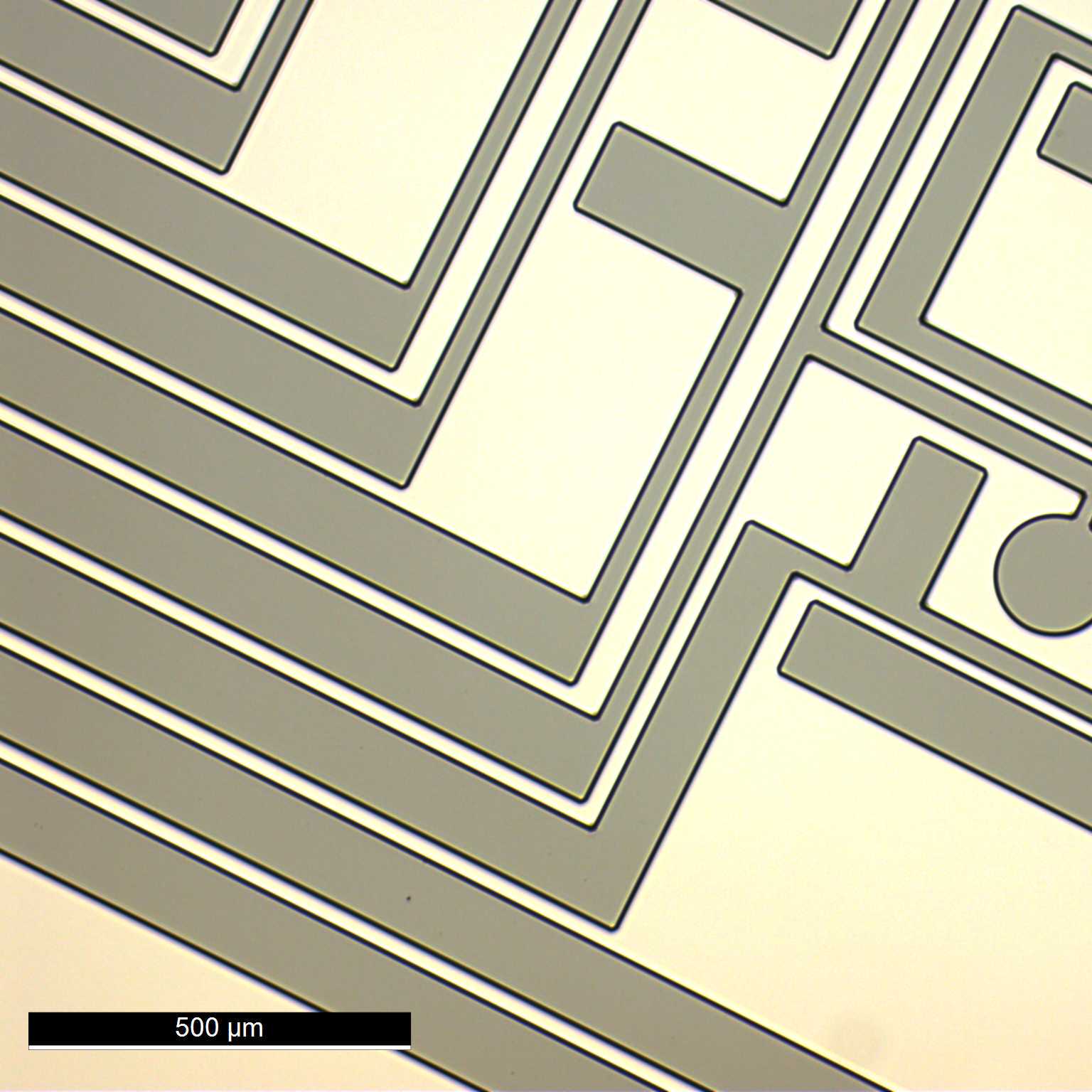
Place the wafer on a hotplate at room temperature, then ramp up to 170 °C (at a ramp rate of ~0.5*C/s). Hold at 170 °C for 00:40:00 , then turn off hotplate and allow to ramp down to room temperature (takes a few hours).
Before reflow
After reflow
40m
Control layer
1h 22m 40s
O2 plasma treatment
Treat with O2 plasma for 10 minutes in barrel asher. (At SMC, Electrotech 508 with typical parameters: forward power 350W, flow 32%, pressure 0.8 torr)
Spin coat with SU-8-3035 (Kayaku) KAM-SU-8-3000-Datasheet-7.10-final.pdf
Spin coat with SU8-3035 using the following programme with ramp rate of 100rpm/s for all steps:
1. 500 rpm, 00:00:10
2. 3000 rpm, 00:01:05 = 25s ramp + 40s hold
3. 4000 rpm, 00:00:01
3. 3000 rpm, 00:00:05
3. 0 rpm, 00:00:30
Make sure the spin coater has a plastic liner installed. If necessary clean back and edge of wafer with wipe soaked in PGMEA.
1m 51s
Softbake
Place on hotplate for 00:12:30 at 95 °C
Let wafer come to room temp (few mins) before exposure. If there are wrinkles, place on hotplate until wrinkles disappear.
12m 30s
Exposure
Expose with the following settings (for a Karl Suss MA8 mask aligner):
Multiple exposure steps: [ 00:00:18 exposure + 00:00:10 wait] x 5 cycles, for a total of 90s (=359mJ/cm^2)
WEC=cont
Expose type = soft
30um alignment gap
5um expose gap
WEC offset OFF
N2 purge NO
28s
Post-exposure bake
a. Place on hotplate at 65 °C for 00:01:00 .
b. Move to second hotplate and hold at 95 °C for 00:04:00 .
5m
Wait for a minimum of 00:10:00 .
10m
Develop
Develop upside down in PGMEA for 00:02:00 , and exchange with new PGMEA for a further 00:02:00 . Check for underdevelopment each time on the microscope (white film). If necessary continue development for up to 6 min.
Underdevelopment after 2+1 min
Correct development after 2+2 min
4m
Rinse with IPA and dry gently with compressed air.
Hardbake
Ramp to 135 °C , and hold at 135 °C for 02:00:00 .
2h
Silanization of wafers
Silanization must be carried out before first use, to prevent PDMS sticking to wafers.
Leave 500 µL of chlorotrimethylsilane (Sigma 386529) in an upturned Falcon cap, inside a sealed box with the wafers until the solvent has completely evaporated.